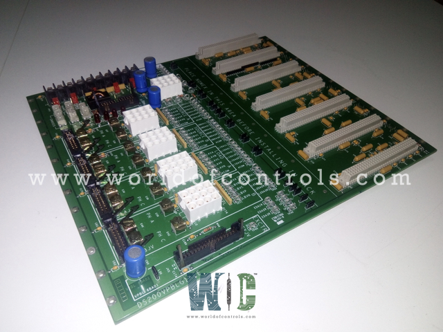
DS200VPBLG1AEE - VME backplane

DS200VPBLG1AEE - VME backplane DS200VPBLG1AEE - VME backplane

World Of Controls understands the criticality of your requirement and works towards reducing the lead time as much as possible.

DS200VPBLG1AEE - VME backplane is available in stock which ships the same day.

DS200VPBLG1AEE - VME backplane comes in UNUSED as well as REBUILT condition.

To avail our best deals for DS200VPBLG1AEE - VME backplane, contact us and we will get back to you within 24 hours.

SPECIFICATIONS

Part No.: DS200VPBLG1AEE
Manufacturer: General Electric
Country of Manufacture: United States(USA)
Product Type: VME backplane board
Series: LCI

DS200VPBLG1AEE is a VME backplane card developed by GE under LCI series. The VME Backplane Board (VPBL) is the VME backplane for the card cage's J2 and J3 sections. The VPBL board is multilayer, with separate analog and digital power planes. Each power connection in each slot has power distribution and bypass capacitors.

DS200VPBLG1AEE Section J2

Section J2 supports the following boards:

  • In slot J1, a Digital Signal Processor Control Board (DS200 DSPC) with daughterboards.
  • In slot J3, to the right of the DSPC, is an I/O extender with daughterboards.
  • In slots J5, J7, and J9, there are up to three Gate Distribution and Status Boards (DS200 FCGD).
  • One exciter board in slot J11.
  • Two spare slots, J12 and J13.

Except for Slot 1, the slot identification number (ID) is permanently hardwired at the P2 connector. Only control signals, such as the 16 MHz clock signal, terminate at the end of slots on the digital bus. The pins in the J2 connectors' B row are only connected to the P5 and DCOM pins.


Section J3

The J3 area is used for external connections that cannot be placed on the board fronts due to space or other constraints. These include current transformer (CT) and burden resister connections, as well as Voltage Scaling Feedback Board (DS200 NATO) connections for the FCGD. The power connections to the backplane are also established in the J3 area. In the J3 area, stab connectors are available for establishing various grounding schemes.

DS200VPBLG1AEE Application Data

I/O Definitions, J2

Section J2 has eight VME-type connectors. Six of them (J1, J3, J5, J7, J9, and J11) have double-wide spacing. J12 and J13 are single-wide spaces that allow for future capability enhancements.

I/O Definitions, J3

  • Diagnostics Connector: DIAGPL is a diagnostics-only 26-pin discrete cable connector. It connects to the processor via I/O on J1.
  • Power / Voltage Analog Signal Connectors: The VPBL board has analog signal connections that indicate the current and voltage status of two source and one load power bridges. Two current transformers (CT) in each bridge are wired through a current sensor interface board and connect to the VPBL board via three Mate-n-LockTM connectors. A voltage feedback scaling board generates the attenuated voltage signals, which are connected to the VPBL board via three 20-pin ribbon connectors.
  • Power connector: For power supply connection, the VPBL employs JAA, a 12-pin Mate-n-Lock.
  • Grounding Stab Connectors: Grounding is established by Stab connectors in the J3 area.
  • Exciter Connection: The signals for an external exciter bridge are handled by a 34-pin ribbon connector called EXJV.
  • Power bugs: Ten power bugs connect the VPBL to the P1 backplane electrically. Because these are on the back side of the board, they are numbered (TB1 - TB10) on the front with reversed (mirror image) lettering.

Testpoints

Sixty spring-loop testpoints allow access to the analog and digital signals generated by the three phases of alternating current on the two sources (input power), as well as the positive and negative dc outputs. Testpoints 55 and 62 - 118 are assigned to J2 connector pins and are only for factory use.

Features

  • TMR controllers receive data from triple-redundant sensors, the number of which varies depending on the system. Because one of Mark V's advantages is its scalability and adaptability, many systems are one-of-a-kind. It is designed to fit into a rack system that accepts and stores other boards. These connect to the eight VME-type connectors on the board's back half. It should be noted that this housing is a separate assembly.
  • The PCB has several vertical pin connectors, including a diagnostic 26-pin discrete cable connector. A voltage feedback scaling board sends attenuated voltage signals to the card via three 20-pin ribbon connectors. The board also has a twelve-pin Mate-n-Lock for power supply connection.
  • On the board, there are three Mate-n-Lock connectors. Tachometer signals are sent to the CPU via a 12-pin terminal block. There are five jumpers and eight stab connectors on the board.
  • The PCB has sixty TP test points. Spring loops provide access to both analog and digital signals. A terminal strip, seven resistor network arrays, four high-voltage electrolytic capacitors, and four LEDs round out the board's

World of Controls has the most comprehensive selection of GE Speedtronic Mark V control components. Our expert engineers are always available to assist you with your Mark V requirements. Please contact WOC if you require any additional information.


Frequently Asked Questions


What is DS200VPBLG1AEE?
DS200VPBLG1AEE is a VME backplane card developed by GE under LCI series.

How to Obtain DS200VPBLG1AEE?
World of Controls provides DS200VPBLG1AEE as well as other turbine control products. Contact WOC.