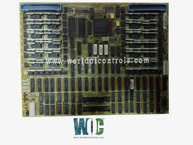
World Of Controls understands the criticality of your requirement and works towards reducing the lead time as much as possible.
DS200TCDAG1AEA - Digital I/O Board is available in stock which ships the same day.
DS200TCDAG1AEA - Digital I/O Board comes in UNUSED as well as REBUILT condition.
To avail our best deals for DS200TCDAG1AEA - Digital I/O Board, contact us and we will get back to you within 24 hours.
Part No.: DS200TCDAG1AEA
Manufacturer: General Electric
Country of Manufacture: United States of America (USA)
Product Type: Digital I/O Board
Availability: In Stock
Series: Mark V
DS200TCDAG1AEA is a Digital I/O Board developed by GE. It is a part of the Mark V control system.The Digital I/O Board, located in the digital I/O cores Q11 and Q51, processes the digital contact input signals from the DTBA and DTBB terminal boards and the contact output (relay/solenoid) signals from the two TCRA boards. The signals are transmitted over the IONET to the TCQC board in R1 and the CTBA terminal board in R5.
The board is an essential component in signal processing, particularly in handling contact inputs from the DTBA and DTBB terminal boards. These inputs are received through the JR and JQ connectors. Here’s a detailed look at how the board processes these signals:
In addition to processing input signals, the board also manages contact output signals. Here’s how it handles these outputs:
The WOC team is always available to help you with your Mark V requirements. For more information, please contact WOC.
What is DS200TCDAG1AEA?
It is a Digital I/O Board developed by GE under the Mark V series.
What is the role of the board in contact input circuits?
The board receives contact inputs from the DTBA and DTBB terminal boards via the JR and JQ connectors. It conditions these signals, assigns time tags to any change of state, and then transmits the signals to the IONET through the JX1 or JX2 connector. Signal inversions for the contact inputs are handled through software using I/O configuration constants.
How does the board condition the contact input signals?
The board conditions the input signals to ensure they are suitable for further processing. This may involve filtering, amplifying, or converting the signals to the required format to ensure accurate and reliable data processing.
What is the significance of time tagging on the board?
Time tagging involves assigning precise time stamps to any change in state of the input signals. This is crucial for accurate monitoring, recording, and analysis of events, allowing for precise tracking of when specific changes occurred.